What is dToF technology?
Recently, Apple Inc. has applied dToF technology for the first time in its newly released iPad Pro device, bringing unprecedented ecological opportunities for 3D imaging technology.
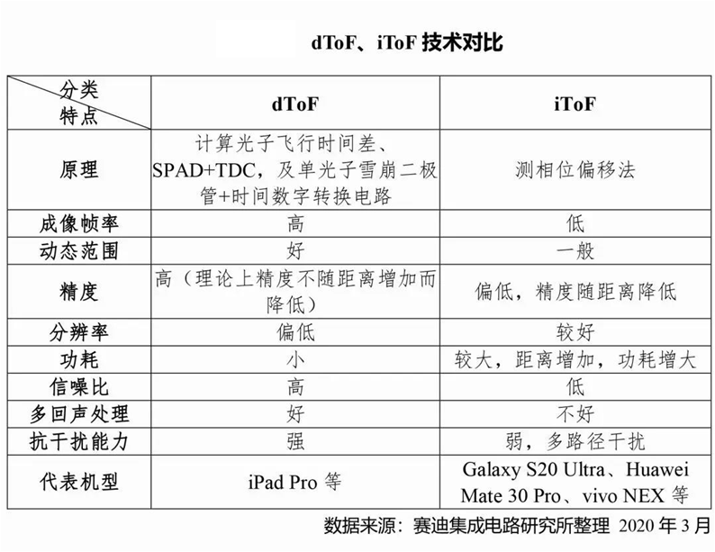
ToF technology can be divided into two types: Direct ToF (dToF) and Indirect ToF (iToF). Among them, dToF sends discrete laser pulses, which can achieve ultra-low duty cycles, are more energy-efficient and have faster imaging speeds compared to iToF, but have higher technical barriers and hardware requirements. Due to its advantages in fast information acquisition, anti-interference, and imaging clarity compared to iToF, dToF is expected to become the mainstream solution for deep sensing imaging technology as algorithm technology and hardware devices continue to mature and improve.
The main difference between dToF and iToF lies in the difference between emitted and reflected light. The principle of dToF is relatively direct, that is, it directly emits a light pulse, and then measures the time interval between the reflected light pulse and the emitted light pulse to obtain the flight time of the light. The principle of iToF is more complex. In iToF, the emitted light is not a single light pulse, but modulated light. There is a phase difference between the received reflected modulated light and the emitted modulated light, and by detecting this phase difference, the flight time can be measured, thereby estimating the distance.
The application of ToF technology not only helps to enhance personal entertainment experience, but may also be seen in various aspects of future work and life. In the near future, ToF technology will rapidly penetrate into personal mobile terminals, and it will further become a high-quality technical solution for application scenarios such as smart payments and smart homes. In industrial, medical, automotive and other fields, the 3D dynamic experience brought by ToF technology makes remote operation more convenient, promoting the intelligence, automation and real-time application of related fields.
How does Changguang Yuanchen provide a backlit solution for dToF technology?
Compared to iToF, dToF performs much better in terms of performance, but its production process is also more complex. Changguang Yuanchen's globally advanced back illuminated CMOS image sensor production line can provide research and development, as well as processing and production services for dToF technology.
Changguang Yuanchen utilizes existing image sensor backlighting technology and improves the sensitivity, temporal resolution, and dynamic range of ToF devices through 3D hybrid bonding. It also solves the serious trade-off between filling print and pixel functions. Compared with other imaging technologies, SPAD has three key comprehensive advantages: single photon sensitivity, picosecond time resolution, and devices integrated in standard CMOS technology. At nanosecond and picosecond time resolutions, detailed three-dimensional (3D) images can be formed by measuring the time of flight (ToF) of light pulses. Single photon high frame rate imaging can generate new functionalities in super-resolution microscopy. In addition, imaging of quantum effects such as photon entanglement can also be achieved.
The main process flow of back illuminated dToF is as follows:
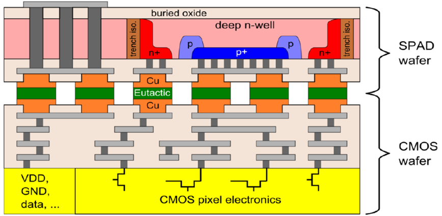
1. Hybrid Bonding
Cu Cu hybrid bonding achieves high-density pixel connections, and this process can reduce the size of pixel units due to the independence of the detector and circuit parts. Changguang Yuanchen can customize Cu Cu hybrid bonding process research and manufacturing according to customer design requirements.
As shown in the figure, the upper wafer is SPAD (including counting and timing), and the lower wafer is the readout circuit l
Cu-Cu互联界面
2. Silicon Thinning
By optimizing the three-step process of mechanical grinding, chemical corrosion, and CMP, precise thinning of wafers can effectively remove internal damage layers and reduce wafer stress.
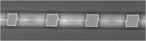
3. DTI
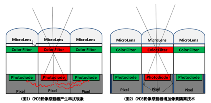
With the reduction of pixel size, problems such as FWC and suppression of crosstalk may occur. FWC can be solved by increasing the silicon thickness, while DTI structure can solve the crosstalk problem. DTI establishes isolation walls to increase light utilization and reduce interference, as shown in the figure:
4. ARC layer sedimentation
By using enhanced plasma vapor deposition equipment, single or mixed deposition coatings can be obtained, and the density and purity of the film layer can be accurately controlled.
5. Pad Open
Changguang Yuanchen can draw and customize lithography plates for customers, ensuring the alignment accuracy of lithography and leaving no impurities in the Pad area.
Changguang Yuanchen will provide comprehensive back illuminated technical support to our customers, helping them fully utilize our technical capabilities and best meet their needs.
About Changguang Yuanchen
Changchun Changguang Yuanchen Microelectronics Technology Co., Ltd. (hereinafter referred to as Changguang Yuanchen) was established on December 29, 2016, with a registered capital of 360 million yuan. Changguang Yuanchen is an independent semiconductor manufacturing enterprise specializing in backside illuminated CMOS image sensor wafer processing. It is committed to providing BSI SOI and special chip level processing services for 200mm and 300mm wafer manufacturing, as well as research and production services for Color Filter&Microlens. At the same time, we can provide customized services according to customer project needs, such as BSI-CIS, Stack BSI, SOI, MEMS, fiber waveguides, 3D ToF, optical thin films (ARC), etc.
The company's main goal is to develop and manufacture back illuminated CMOS image sensor chips for mid to high end applications, providing solutions that meet the manufacturing needs of customers for mid to high end CMOS image sensors. In the future, it will build an integrated semiconductor enterprise that integrates design, manufacturing, and packaging testing, providing highly competitive high-quality products and services for global customers.