


Core technology
Hybrid Bond & Fusion Bond
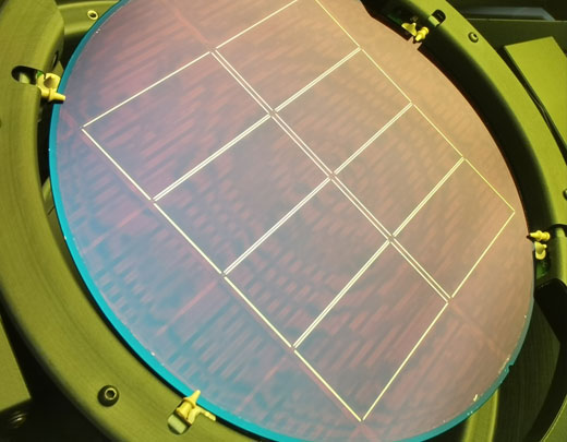
YCMEC owns a complete 8-inch BSI product processing line, covering all processes including bonding pretreatment, bonding, anneal, thinning, wet etching, CMP, ALD, ARC, and Pad Open. This full-flow process capability significantly enhances the quantum efficiency of image sensors.
| Project | Capability |
| Bond force | ≥1.8J/m2 |
| Empty | ≤0.5% |
| Alignment accuracy | ≤800nm |
| Thinning TTV | ≤3um |
| Final TTV | ≤0.5um |
| ARC uniformity | ≤3% |
| Pad Open accuracy | ≤2um |
-
Wafer informationThe customer provides CIS and Handle wafer
-
CharacteristicHigh alignment accuracy up to 800nm, CIS requires customers to provide surface planarization wafers
-
Technological processWafer bonding+wafer thinning+ARC layer deposition (Pad Open process can be developed)