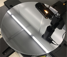


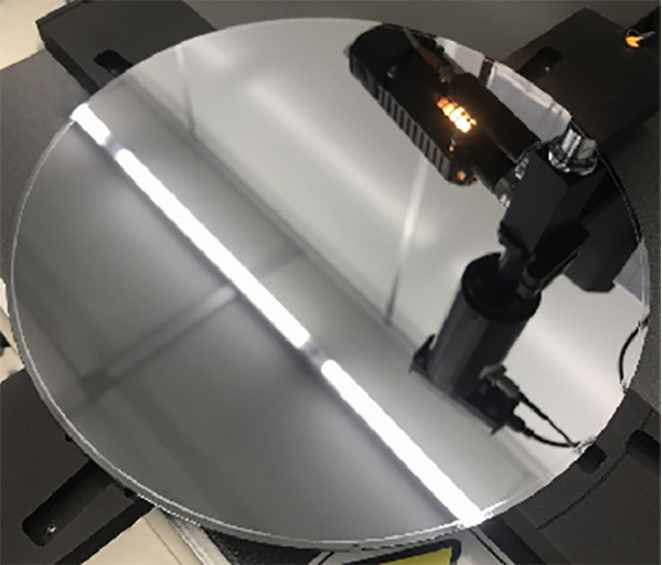
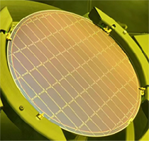
BSI Wafer Processing
8 inch BSI Wafer Processing:Fusion&Hybrid Bond
Bonding accuracy:3σ≤800nm(depends on wafer)
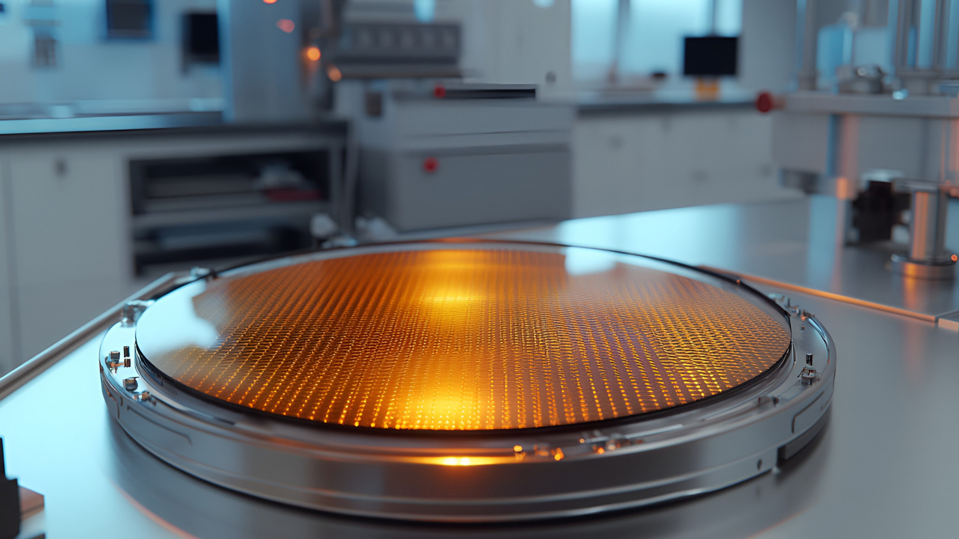
12 inch Wafer Processing:Fusion&Hybrid Bond
Bonding accuracy:3σ≤500nm(depends on wafer)
BSI Product Process
|
8 inch Fusion Bond |
12 inch Fusion Bond |
12 inch HYB Bond |
|
Wafer Trimming |
Wafer Trimming |
Surface Treatment |
|
Wafer Fusion Bonding |
Wafer Fusion Bonding |
Cu electroplating and CMP |
|
Wafer Thinning |
Wafer Thinning |
Wafer Hybrid Bonding |
|
Wet Etch |
Wet Etch |
Wet Etch |
|
CMP |
CMP |
CMP |
|
ARC |
ARC |
ARC |
|
Pad Open |
Pad Open |
Pad Open |
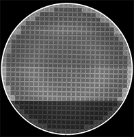
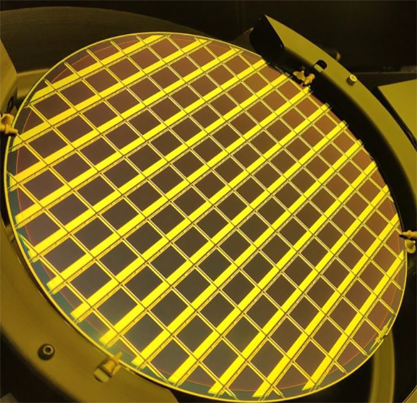
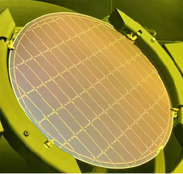
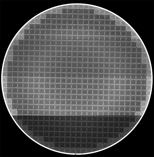
8 inch Wafer Products: YCMEC has offered 8inch BSI wafer processing to a wide range of domestic and international customers. Our services cover diverse Si thicknesses, anti-reflective coating (ARC) structures, and die sizes, with stitching process capability.
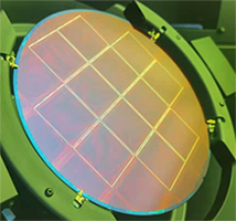
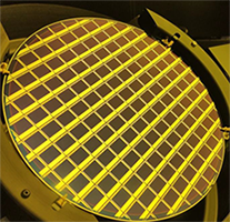


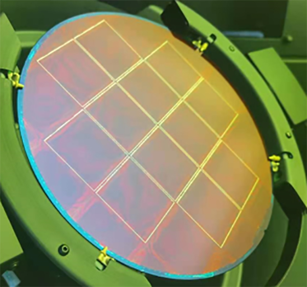
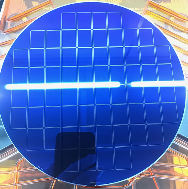
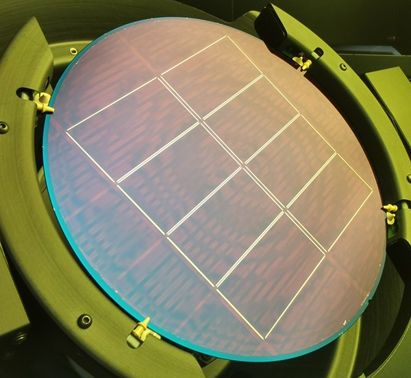
12 inch Wafer Products: YCMEC has BSI process capabilities for 12inch Fusion Bond and Hybrid Bond, as well as bonding capability for products of various sizes.